


When evaluating NAND flash-based devices as the storage medium for an embedded application, factors such as the host interface(s), power consumption, physical space, performance, capacity, environment and cost will often dictate the selection. Endurance requirements are also a major part of the decision, and as we will discuss, the program/erase (P/E) cycle rating of the raw flash die is only one piece of the puzzle. How the device is written to – in terms of both the controller technology and the application workload – have a significant impact on the TBW and resulting life of the drive.
RAW FLASH ENDURANCE: SLC VS. MLC VS. pseudoSLC VS. TLC
The first factor affecting drive TBW (TeraBytes Written) and useful life is the endurance rating of the raw flash – how many times a block can be reliably written to and erased. There are three basic classes of NAND – single level cell (SLC), multi-level cell (MLC) and three level cell (TLC), all based on the same fundamental technology, but with significantly varying endurance based on the number of possible states and the resulting margin of error. By virtue of the physics of these designs, SLC is the most robust, but also the most expensive – and is therefore typically used in applications that log mission-critical data, launch an operating system or an application, but quite frequently, a combination of these functions. MLC is gaining more traction in the industrial embedded space for less write-intensive applications or where larger available capacities can offset the need for higher P/E cycle ratings. MLC can also be used in pseudoSLC or pSLC mode for increased endurance and write performance over standard MLC. There are two primary methods of implementing pSLC – “true” pseudo mode, whereby the controller utilizes flash commands to alter voltage thresholds of MLC cells, and “fast page” (also referred to as “strong page” or “lower page”) where the standard MLC voltage thresholds are utilized, but only on the lower page of each cell. Both methods halve the usable capacity of the MLC flash, with varying endurance and performance, yet provide a solution that is between standard MLC and SLC in terms of cost and durability. TLC, however, is mainly used in consumer applications that are not heavily taxing relative to the frequency or volume of data written.
When determining the type of flash that is best suited for a given application, endurance and robustness are key attributes to evaluate, however the raw flash specs are not the only factor in overall drive life.
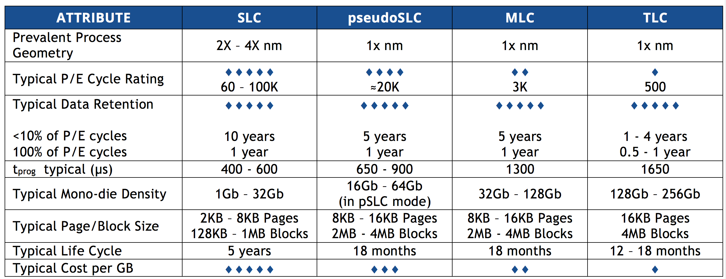
TABLE 1: COMPARISON OF RAW FLASH TYPES
Note: The data in above table serves to illustrate the relative characteristics for the various flash technologies, and does not represent any specific flash components.
CONTROLLER TECHNOLOGY – IMPACT OF TYPE AND FIRMWARE ON ENDURANCE
The basic architecture of NAND flash dictates that the smallest possible unit for programming is a single page, whereas for an erase, the unit is a whole block. However, depending on the controller type and technology, the smallest flash unit for write activity can also be a full block. Generally speaking, if a flash device has a separate DRAM component (most SATA form factors, for example), the page is the smallest unit for writing.
However, if a card or drive does not contain a DRAM (such as SD cards, USB drives, CompactFlash cards), then typically most controllers are block-based and will consume a whole block even for a very small write. The impact of block-based firmware is a potentially higher Write Amplification Factor (WAF) which consumes P/E cycles and wears out the drive more quickly. Page-based mapping is most impactful for MLC flash configurations, where the pages are larger, blocks contain more pages and endurance is significantly lower. Page-based mapping is less relevant for SLC, which already has very high endurance, along with smaller page and block structures.
To illustrate the effect of block versus page-based writing on an MLC card:
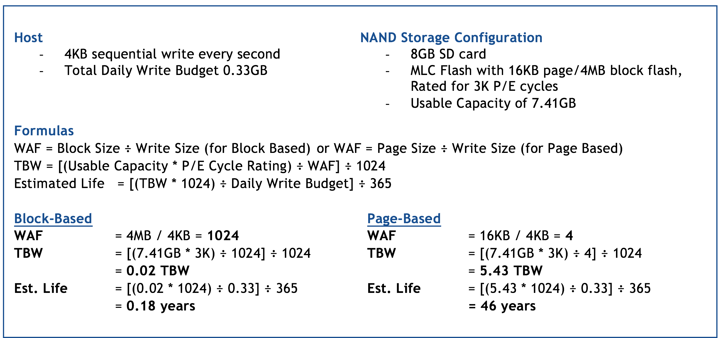
EXAMPLE 1: BLOCK-BASED VERSUS PAGE-BASED
As illustrated, understanding the controller mapping technology relative to the flash structure is another key factor in endurance. Additionally, controllers and firmware developed for industrial use often have features and capabilities to address the varied usage models, platforms, operating systems, etc. employed in embedded applications.
This is in contrast to the technology utilized in retail-grade products, which are highly cost-driven and aimed at general consumer use with much less taxing workloads and lower endurance requirements. This leads us to the final piece of the endurance puzzle, the usage model and workload.
USAGE MODEL IMPACT ON FLASH LIFE
The write profile of a host application – in terms of transfer sizes, frequency of writes, number of data streams and the sequential vs. random nature of the data – has a major effect on the consumption of P/E cycles the resulting drive endurance. The most efficient write model, in terms of maximizing flash life, would be sequential block-sized data transfers (or page-sized in cases where the controller can manage writes at that level.) However, as block sizes are 128KB at a minimum and 4MB at the high end, it is rare that an industrial embedded application would consolidate or buffer that much data for a single transfer. The operating system may also break up the transfers into smaller chunks, unbeknownst to the user.
The worst case workload scenario, in terms of flash endurance, would be frequent, small, random writes – whether there are multiple streams writing to different partitions or simply data file updates of a few bytes at a time.
Similar to the example of page versus block-based controller firmware, the next example models small frequent writes as opposed to larger consolidated writes for the same 8GB MLC SD card:
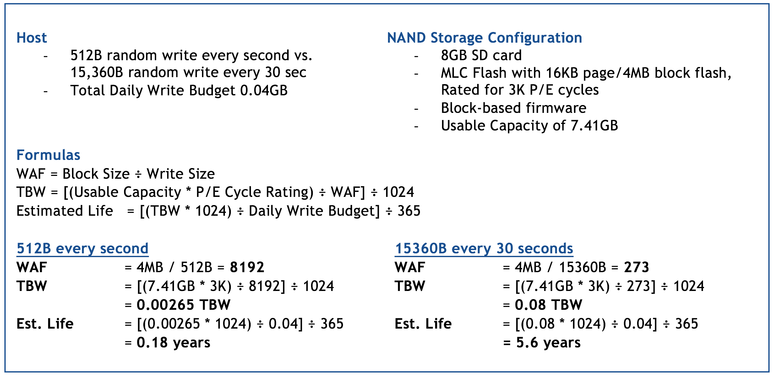
EXAMPLE 2: SMALL RANDOM WRITES VERSUS CONSOLIDATED WRITES
Understanding the workload, along with the endurance and lifetime targets, can assist in selection of the optimum storage product solution.
In conclusion, with a wide array of interfaces, form factors, flash types and controller technologies available in the NAND flash storage arena today, there are a multitude of possible combinations and solutions available. In order to select the optimum drive that meets the endurance targets and budget for your industrial embedded project, there are several key factors to consider – including the characteristics of the raw flash, the controller technology and the application workload.
Contact us to discuss your latest project, and let our technical and applications staff assist in identifying the ideal Delkin Devices storage solution. All Delkin industrial products include controlled configurations, managed life cycles, customization options and consistently high quality, delivered by our US-based design, manufacturing and support teams.