


SSD NAND Flash- Wear Leveling and Maximizing SSD Life
This paper will describe NAND Flash life as used in Solid State Storage Devices.
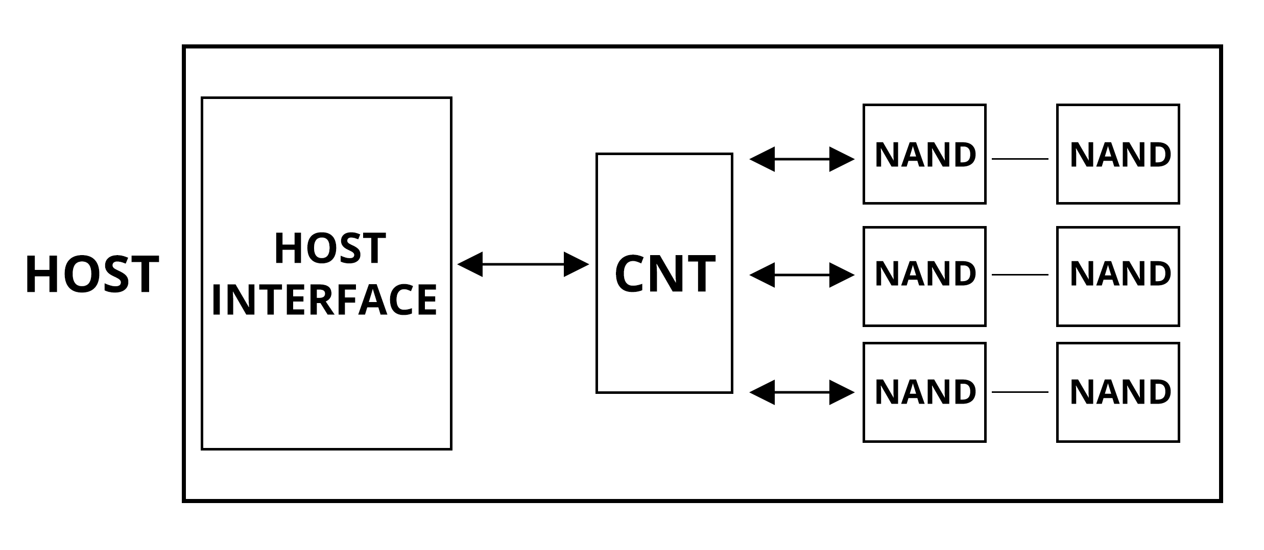
SOLID STATE STORAGE
These Devices consist of Disk Drives, Compact Flash Cards, SD/MMC cards, USB sticks and custom storage modules.
Aside from differing host interfaces, all these devices share common items:
- Multiple NAND Flash devices
- NAND Flash Controller with Firmware
- Support Circuitry
NAND FLASH CONTROLLER
These are ASIC devices generally containing, at a minimum:
- CPU with ROM BIOS
- Ram Memory
- Flash Bus Interface (single or multiple channel)
- Application specific host interface (USB, SATA, PATA, PCI Express, SD, MMC).
NAND FLASH TYPES AND FLASH BASICS
- SLC (1 bit per cell) – fastest, highest cost – 100K P/E
- eMLC (2 bits per cell) – faster than regular MLC – Enterprise MLC – 30K P/E
- MLC (2 bits per cell) – Slower Than SLC – Higher Density – 10K P/E
- TLC (3 bits per cell) – Higher density than MLC – 3K PE
- QLC (4 bits per cell) – slowest, lowest cost – highest density
- 3D Flash – Fast – expensive
WRITING NAND FLASH
NAND Flash chips are made up of blocks of cells. Blocks consist of multiple pages. Pages consist of multiple sectors.
Writing to NAND Flash can only be done at the page level. Pages must be written sequentially. In all but SLC, pages can only be written once. Erasing can only be done at the block level. Because of this, the Flash controller FW has a very complicated job.
NAND FLASH ENDURANCE
Flash blocks don’t have infinite life. MLC blocks, for example, may have a limit of 3K program/ erase cycles. When this limit is reached on a block, the block is not useful anymore. It may experience program/erase errors as well as read errors.
In practice, these blocks are picked up by bad block management, and are mapped out and replaced by spare good blocks.
SSD ARCHITECTURE
All SSD devices contain a Flash Controller. Most SSDs contain multiple NAND Flash chips. This is key to performance and equally as important, for device life.
Key to device life, is a high degree of parallelism during writes, by spreading data across multiple Flash chips. This can be done in several ways. Many controllers have multiple Flash bus channel support. This allows spreading data across the Flash connected to each channel. In addition, data can be interleaved between chips on each channel.
By doing so, this is one of many ways of taking the stress off a single chip. In fact, the more chips used, the longer the device life. As we will see chip density is one factor in device life.
CONTROLLING FLASH WEAR– FTL (Flash Translation Layer)
The most critical part of controller firmware is the FTL. There are several reasons for this. Not only does this determine device performance, but it determines device life.
Why is this? The answers are simple. The mapping scheme used determines a key factor in device performance and device life. This is known as Write Amplification Factor or WAF. As we will see, WAF directly factors in to device life. WAF is a ratio of device writes to internal Flash program/ erase cycles. Ideally this ratio is equal to 1. This can be approached but never happens continuously.
FTL mapping schemes are a big factor in device life. The 2 basic block logical to physical mapping schemes are Block based and Page based. Page based mapping is more complicated, takes more RAM and requires a defragmentation generally termed “Garbage Collection”. However, it yields faster write speeds and much lower WAF. Lower WAF translates to less block erases and thus longer device life.
An absolute requirement of the FTL is wear leveling. Wear leveling insures all Flash chip blocks receive similar amounts of P/E cycles. This is important as it reduces the possibility of a single block affecting the drive life.
Static wear leveling is by far the best and most used. This type of wear leveling uses all available Flash blocks in the wear level. So blocks that are rarely written are swapped as well. This goes a long way in adding to drive life.
The majority of SSD devices use multiple NAND Flash chips, as indicated earlier. Data is written across all chips. Wear leveling is generally applied within each Flash chip, because swapping blocks across Flash chips degrades performance. As a compromise, wear leveling is performed within each Flash Chip, until any one Flash Chip has reached a fixed percentage of its maximum P/E Cycles. At that point wear leveling is switched to swap blocks between all Flash chips. The SSD slows down, but its life is extended enough until it can be replaced.
ASSESSING SSD LIFE
To summarize, these are the factors affecting SSD life:
- SSD Density- the higher the density, the longer the life
- FTL Architecture
- Logical to Physical mapping schemes
- Page based mapping = less block erases
- Wear Leveling – Static is best -all blocks cycled for even wear
- WAF – as close to 1 as possible
- Flash Type
- SLC has the longest life at 60K to 100k Block P/E cycles
- MLC has a typical life of 3k to 10K
BENCHMARK USED FOR SSD ENDURANCE
The most used benchmark for SSD endurance is TBW or Terabytes written. This simply indicates the amount of data that can be written to the device until it is no longer useful.
TBW is a function of drive capacity (bigger is better), WAF, WLF (Wear Level Factor), NAND P/E cycles. WLF is and indicator of wear leveling effectiveness. Static wear leveling approaches a value of 1.
TBW = Capacity * P/E / WLF * WAF
TBW is the base of dynamic monitoring of drive life remaining.
As an example, let’s take a 2 TB SSD and calculate TBW for this device using 30K P/E cycle eMLC a WLF of 2 and a WAF of 5:
TBW = 2 *30000 / 10 = 6000 TBW
So, we can write a total of 6000 TB to this 2 TB drive until it is near or at its end of life.
We have a WAF of 5 and WLF of 2 to be conservative. SSD devices with properly designed controllers will do better.
By monitoring daily writes to the SSD, Percent Drive Life remaining is possible. This is in fact done by many SSD devices and stored in SMART data. This is retrievable by the host using SMART commands.
So how long will this SSD last? It depends on how much data is written to the drive per day. If we write 100 GB of data per day, this drive will last 6000 / .1 = 60000 days = 16.43 years. Naturally the manufacturer will specify a shorter warranty period, 5 Years is typical.
SMART DATA
Device status, including % remaining device life is available in SMART data. The actual drive life data is constantly changing based on daily written data. It can be checked regularly by the host.
CONCLUSION
The days of considering the SSD inferior to the HDD are over. Almost all laptop devices and even most desktops use SSD storage. Constantly improving Flash devices and highly sophisticated Flash controllers make this possible. Highly sophisticated FTL designs allow for very high magnification of Flash life. With increasing Flash densities and the advent of 3D flash, very large drive densities are possible. All this makes for very reliable and long-life cycle SSD devices without the mechanical issues of the HDD.
ORDER DELKIN INDUSTRIAL FLASH STORAGE TODAY through our distribution partner Newark.
Contact
Article Contributor:
Carmine C. Cupani, MSEE
CTech Electronics LLC