


NAND Flash 101
NAND Flash Introduction
Technological advancements over the last forty years have moved at an accelerated rate the scale of which has never been seen in human history. It is estimated that 90% of all the data ever created has been created within the last two years. Computing and processing power has grown exponentially as has the amount of data we create, store and communicate globally. The amounts of data we can share and the speeds at which we can transfer it were impossible just a few years ago. Advancements across multiple technology platforms have made this all possible. One such technology is NAND Flash and the related memory storage products that are built using it.
Simply put, NAND Flash is a type of memory that can maintain the data stored within its’ cells even when there is no power being provided to the storage device. For this reason, NAND Flash is known as “Non-Volatile” memory. NAND Flash is also “Solid-State” memory in that the individual NAND die and subsequent NAND based module form factors have no mechanically moving parts. No moving parts means there are no parts to break or physically wear down. These combined assets make NAND Flash memory the solution of choice for key process functions and as the primary memory in many specific end applications. NAND Flash based storage is the consummate solution for boot & cache functions as well as for today’s demands of the mass storage of images, videos and music in a portable device such as a smartphone. Industrial Grade NAND Flash is the solution of choice for applications working in harsh environments or mission critical applications where the results of data loss or memory failure are catastrophic.
NAND Flash Development & Utilization
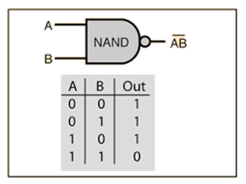
NAND Flash was developed in late 1980’s and is credited to Fujio Masuoka while working for Toshiba. Masuoka was able to leverage existing floating gate technology being used in rudimentary storage solutions such as EPROM’s and EEPROM’s to develop a storage cell with the ability to store and subsequently erase larger sets of data all at once, or in a “flash.” As such, the name “flash memory” was born. The memory industry is full of acronyms but “NAND” is not one of them. The name NAND is a Boolean expression for the binary inputs that make NAND Flash operable and equates to “NOT AND,” i.e. you only get a FALSE value when both inputs are TRUE. This creates binary’s subsequent 1 or 0 values.
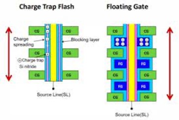
There are two methods that can be used to build a NAND storage cell: “Floating Gate” and “Charge Trap.” Floating Gate NAND maintains original design methods and uses a “doped” polycrystalline silicone layer to store charged electrons. Charge-Trap technology was not commercially utilized until after the year 2000 and uses a silicon nitride film to store charged electrons. Charge-Trap NAND allows raw NAND manufacturers to utilize smaller process geometries, has lower programming voltage requirements and at face value, provides higher reliability. Floating Gate technologies have shown similar capabilities in recent years through the use of “tunneling.” Both technologies result in the same thing; a memory cell that can store electronically programmed bits of data, then erase it and repeat the program and erase cycle multiple times.
It can be confusing to understand the broad spectrum of NAND based storage solutions and the differences within all the variables that make up the range of options in the market today. Managed NAND solutions that are packaged in popular form factors such as microSD Cards, or 2.5” SSD’s look the same, and in fact are the same from the standpoint of their size, connector pin-outs and other features that meet industry developed standardizations. However, the differences inside those form factors and the respective NAND die that work within them have a wide expanse and it is important to understand their many differences. For example, the microSD card you buy for a digital camera at a big box store is not “the same” as the microSD card you buy for use in an industrial computer. Even though the cards look the same, are the same size, have the same connectors and in fact will fit into the same sockets, they will not perform the same and do not have the same reliability, longevity, or intended use.
NAND Flash can be utilized in two forms: Raw NAND and Managed NAND. Raw NAND is used at the individual memory die level and requires external support technologies to enable the NAND die to perform. These functions include wear leveling, bad block management and ECC (Error Correction Code) that are handled by a controller in a Managed NAND solution. Managed NAND is Raw NAND that is utilized within a module form factor that has been specifically designed to support a wide range of applications. Managed NAND solutions include the controller / firmware technology embedded within the module to manage all the key NAND background operations and do not require additional support technologies the way Raw NAND does. Managed NAND storage solutions utilize multiple, individual, NAND die within the module which drastically increases the available storage capacity, or density of the Managed NAND solution. When partnered with a controller optimized for Industrial performance, Managed NAND storage in its’ many form factors also allows Industrial NAND providers such as Delkin Devices, to provide value add features enhancing the longevity, performance and ruggedness of the module as well as improving resistance to dust, water, and corrosive air environments.
NAND Flash Architecture
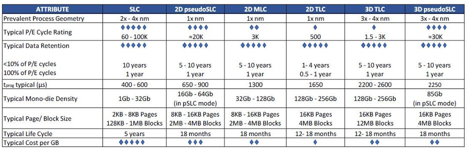
NAND Flash can be built using different architectures of design on the Raw NAND die. These architectures include SLC (Single Level Cell), MLC (Multi Level Cell), TLC (Triple Level Cell) and QLC (Quadruple Level Cell) designs. Each architecture has benefits and trade-offs and is designed for use in different applications and operational environments. For example, SLC NAND provides the highest reliability in data integrity and device longevity in terms of Program / Erase cycles but is also the most expensive NAND option and offers a relatively lower storage capacity. On the other end of the spectrum, QLC NAND offers extremely high storage capacity at a low price-point, but it is weak in terms of reliability and longevity. Choosing the Managed NAND storage solution built from the NAND die architecture best suited to your application is paramount. It is also wise to consider the T.C.O. (Total Cost of Ownership) of your Managed NAND solution. Following the adage “an ounce of prevention is worth a pound of cure,” – if the costs of bad /incorrect data storage or outright failure of the memory in your application are high, it is better to invest in a high reliability NAND die design such as SLC up front than to pay the exponential costs of failure down the road.
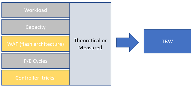
NAND Flash architecture has recently undergone the largest industry wide advancement in its’ history; the development of 3D NAND. Prior to 3D NAND, all NAND die architectures were “Planar” designs and stored data only one dimensionally. 3D NAND designs allow for the NAND cell to store data vertically in layers as well as one dimensionally within the cell. Imagine a city block with single story apartment units built on it and how many people can live within those apartments. This would be a Planar NAND design. Now imagine the same city block but on it we can build multiple story apartments on the same physical space and how many additional people can now live there. This would be a 3D NAND design. The advantages in terms of “how much” can be housed or stored within a certain, physical space are clear. This advent has changed the lowest capacity available in several form factors as with 3D NAND it simply does not make sense to produce lower capacity cells when you can produce higher capacity cells for the same cost on the same physical footprint. 3D NAND improves the over-all TBW (Tera Bytes Written) of a like design using 2D NAND because the page and block size of 3D NAND is superior. Write amplification must be factored in when calculating the actual life cycle of 3D storage solutions. The experienced, U.S. based FAE team at Delkin Devices can provide accurate life-cycle modeling for 3D NAND designs within your specific usage model.
Controller and Firmware advancements have also added to the confusion in determining which NAND storage solution is the best choice for your application. Controllers can make the relative NAND die “behave” as if it is a different die architecture. There are many names for this functionality, the most common being pSLC or “Pseudo-SLC.” Pseudo-SLC based options use the controller to manage the storage of data in such a way that the memory device can provide additional performance, reliability, and longevity but this comes at the expense of the usable capacity of the storage device. For example, a 3D pSLC based microSD card uses 3D TLC die. By using the controller to overprovision the way the data is stored the microSD card will see an increase in its’ reliability but also see a reduction in its’ storage capacity. A card operating in its standard mode would have, say, 64GB of capacity but when the controller makes the card operate as pSLC, the capacity of the card will only be 16GB – 20GB, depending on the firmware in use. While a pSLC solution still does not have the over-all reliability or longevity of an SLC cell, it does provide an improvement over a standard 3D TLC cell and is offered at an in-between price point. Differences in NAND architecture, design process geometries and the respective performance and lifecycles of each technology:
Choosing a Managed NAND storage solution based on the architecture best suited for your end application is the key to long term success for industrial designs.
Industrial Applications
Many of the technological advancements of the last 3 decades have centered on portability, removability and the increased storage capacity of the memory utilized inside the product. This data must be stored remotely, while still being stored reliability and securely. This makes NAND Flash based storage a perfect fit within the larger technological landscape of today’s devices and industrial applications. NAND Flash has become the key memory technology of choice to meet these needs while also meeting the needs of capacity, cost per bit, reliability of data storage and longevity of use. NAND Flash used in its’ many module form factors is an ideal solution vs. Raw NAND because the controller and firmware management of the storage solution is already managed within the device, eliminating the need for external, secondary management of the memory. NAND storage solutions are not “one size fits all.” Choosing memory experts like Delkin Devices who will partner with you long term and help guide you through the NAND landscape to choose the best NAND Flash based storage solution for your application is imperative to design success.
For more information and specific NAND Flash based product information, please contact Delkin Devices at delkindevices.com.
ORDER DELKIN INDUSTRIAL FLASH STORAGE TODAY through our distribution partner Newark.
For Europe Contact Our Partner Farnell
Contact