


Industrial Flash Drives – Framework & Composition
Introduction
Industrial Flash drives, no matter the form factor, are more complex than meets the casual eye. A Flash drive consists of two major parts. One part is, of course the Flash chips, and the other part is a highly integrated controller chip, or CPU.
This article will focus first on basic Flash architecture, operation and how it can be configured in different ways with the CPU to achieve different performance speed goals.
Flash Storage Data Structure
All data whether it is an image or highly encrypted classified information can be reduced to its lowest level, the bit. These bits can then be stored electronically on any media whether it is magnetic tape, spinning hard drives or Flash drives. A bit, the smallest storage element, is stored as either a 1 or a 0. A bit on its own is not terribly useful, but when formed into a group of 8 it represents a byte of data. All data can be can be broken into bytes. Bytes are the universal storage element of all recordable/storage mediums.
Flash Cell Pages and Blocks
A Flash cell consists of a transistor that stores energy and this stored energy can translate to a 0 or a 1. Based upon the way the energy is stored, a single transistor can store from 1-bit (single level cell (SLC) 2bits multi-level cell (MLC) 3bits tri level cell (TLC) and 4 bits quad level cell (QLC). These microscopic transistors are the building blocks for all Flash used in drives today.
A single cell of Flash is not of much use on its own. It must be arranged in a way actual data can be stored and retrieved logically. Cells, or bits, are arranged into groups of 8, or bytes. These bytes string together forming words of many bytes. These words are then arranged in rows producing a page of data. These pages range in size from 1K bytes to 128K bytes. These pages are then arranged into blocks which is the final unit of measure that most Flash operations work under.
Even though the block has been constructed as described, the size of one block is still considered relatively small, up to 2MB in some cases. A NAND chip consists of an array of blocks which is typically accessed as a single unit. A drive may consist of a single NAND chip or many NAND chips depending on the application capacity and speed requirements.
Flash Drive Usage Models
The two extremes of usage models of Flash drives are:
1)very low cost, moderately low capacity and moderate to low speed
2) extreme high speed and high capacity.
All along this continuum is where most drives fall.
To reach each of these desired product goals, many things can be done via the Flash chip configuration but, each has a tradeoff, for example:
A small capacity device, say 8GB, might be achieved with a single 64G-bit chip. This single Flash chip is connected directly to the CPU’s pins and all transactions take place with this part. Because of this configuration choice, the cost to manufacture this device is very low and the performance will not be as strong.
Read/ Write Capabilities and Interleaving
To Read or Write to a Flash cell, takes time. The cell must be either programmed or read back by the CPU. Each of these operations have a set time to complete. Reading is much faster than writing since the blocks of cells must be erased and then reprogrammed.
Taking the same 8GB capacity drive, if built with 2 32G-bit chips, the same capacity is achieved but the cost is slightly higher since multiple parts are used. Each of the 2 chips are connected to the same channel on the CPU. This allows the CPU to interleave the data between the two chips. Interleaving is the concept of having multiple chips which can perform functions in parallel. The firmware in the CPU, virtually grouping the blocks together into Super Blocks, keeps track of where the data is and how it is spread across the two chips. By doing this, the CPU can start and erase on one chip while it is writing data to the other, thus cutting the write time virtually in half. The cost of the drive is only driven up due to the extra Flash chip with no enhancements to the CPU hardware.
Multiple Channels of the CPU
Extending this principle of interleaving farther, if the CPU has multiple channels, the same 8GB drive using 2 32G-bit chips, each chip can be read and written to at the same time, thus twice as much data can be transferred on a read as the CPU with a single channel. This additional channel on the CPU will drive the cost up further as it is a more complex and physically larger component.
Using the interleaving idea on a 2 channel CPU, if 4 16G-bit chips are used to make the same 8GB drive, you can see the advantage of having 2 channels and 2 chips on each channel. This provides twice the data transfer plus being able to interleave write and erases.
As flash chips grow, 16G-bit chips become unavailable, causing the smallest capacity of drives to grow, also causing performance to be reduced since fewer chips are used for small capacity drives.
High Performance Flash Drives & Superblocks
In very high performance drives a CPU can be made with 4 channels supporting 2 or even 4 chips per channel. This will prove to enhance performance by many orders of magnitude since the firmware is able to access a super block as one unit. Multiple levels of interleaving are now available with the multiple channels and multiple chips per channel.
These Super blocks, at the discretion of the firmware developer, may consist of all blocks at a single address on all channels. The superblock may be also extended to include all blocks at the address on all channels and the corresponding interleaved blocks on the same channels.
However, due to this arrangement, the manufacturer is unable to achieve these ultra-high speeds on lower capacities since it requires 16 chips to fully realize the speed advantages of multiple interleaves on multiple channels.
This example also introduces complexity into the CPU firmware since data must be managed across many chips holding consolidated data.
Flash Drive Wear Leveling
One factor in this complexity is that Flash cells do not last forever, they do wear out. The “wear” is caused by the erasing and reprogramming of data. When a cell is no longer able to hold data, it is marked as “bad”. However, not just the single cell, but the entire block where this or multiple bad cells reside. Due to the way the super block is arranged, it is often required to mark all the blocks arranged in the superblock as bad since one is bad. This will result in many blocks that are not bad to be retired along with the one that is bad due to the way the superblock is constructed in the drive firmware.
The drive firmware consists of many more elements that just the reading and writing of user data to the Flash. One aspect is the management of the wear on blocks, called wear leveling. Since blocks are susceptible to wear, the firmware controls which blocks are used so that each block is erased and reprogrammed uniformly. This is done in several steps.
- A counter is kept for each block indicating number of erases that have been performed
- A table is kept which maps which physical Flash block or superblock translates into the correct logical block. Meaning, the host computer may write to logical block address (LBA) 0 very often, but each time the data is stored into a different super block thus allowing the Flash chips to be used uniformly. This prevents early failure of a few blocks which would be mapped to commonly used LBA’s.
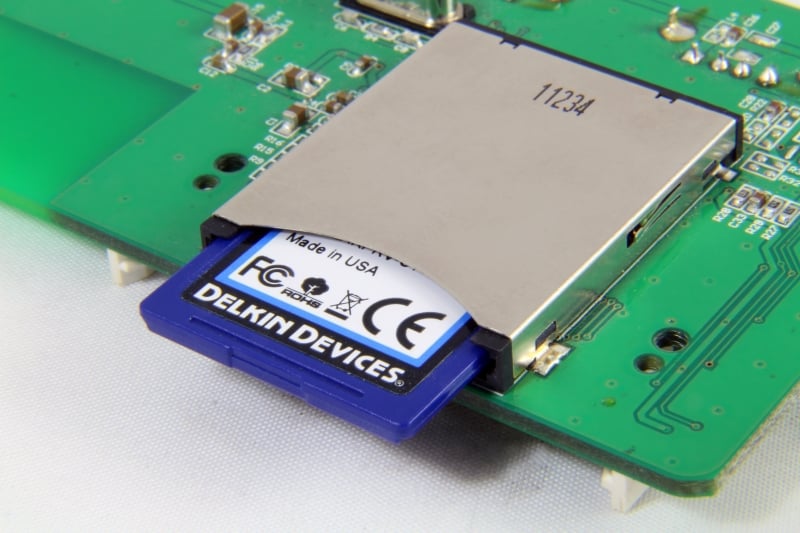
Delkin Industrial Flash Drive Quality
All Delkin Flash storage products have a very high level of firmware complexity to support wear leveling and the other facets of the firmware. High end storage devices made by Delkin Devices are able to achieve the highest level of performance by employing all of these chip and interleaving concepts.
Delkin offers industrial grade flash drives with capacities ranging from 128MB to 32GB and a number of customization options. Discuss your storage needs with our product team today to see what flash drive is right for you.