Flash Storage Deconstructed- Improve Write Life with Simple Changes
Anatomy of a Flash Storage Device
To the casual user, a FLASH card seems like the perfect simple device that you can write to as much as you need, and it remembers the data when you power it off. This is true in the simplest form; however, FLASH technology requires a CPU with highly complex firmware onboard to manage the device interface and the complex challenges of FLASH memory chips. Neglecting this advanced firmware can lead to early failure and lost data.
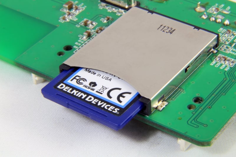
A FLASH card, whether it be an SD, USB, CF, or SSD, etc. are all built with FLASH chips, and a controller to manage the data between the interface and the FLASH chips. This CPU as mentioned contains the complex management firmware required to maintain and retain data.
How Data is Written to Flash Storage
A typical FLASH chip is constructed by grouping cells into “pages” of 4K or 8K or higher cells. These pages are then grouped into blocks of pages anywhere from 256 pages to 16K pages depending on the FLASH chip. Thus, a single block can hold a large amount of data. The CPU firmware groups these blocks together and maps the card’s external Logical Block Addresses (LBA) to each FLASH block.
One important constraint to note about a FLASH chip is that only an entire page can be written at a time. Thus, if a small amount of data is written, there is space that is left over in the page.
Flash Storage Erase Cycles
Another important constraint is that the block is the smallest unit that can be erased in a FLASH chip. This means that to change even the smallest data in a page, or pages in one block, the entire block must be erased first.
One final constraint to note is that each block has a limited number of erase cycles, depending on the FLASH technology it can be anywhere from500 (TLC) to 3000 (MLC) to 60,000 (SLC) cycles. As the device nears its erase cycle limit, the device tends to have a shorter retention time. To avoid this, the CPU has firmware onboard that attempts to keep all blocks at the same erase level, or wear level, to ensure that the device can be used for the longest time.
Write Amplification Factor
With all this in mind, when a few bytes in a single page needs to be updated or added to, the existing data must be moved to a new block along with the updated data. After this move is complete the previous block is marked to be erased. This moving of data means that the same piece of data is written many times over and over as the data is moved from one block to another to facilitate updates and changes. This is referred to as Write Amplification Factor. The smallest the WAF can be is 1 if the data is never moved, and only grows from there. The higher the WAF, the more inefficiently the card is being used.
“Block Based” Firmware
In the case of an SD or USB card which have less powerful controllers, the firmware used is referred to as “Block Based” in that data is stored in as many pages as needed for that single transfer and then the remainder of that block is not used. The subsequent transfer will utilize another set of pages in a new block. When there are no more blocks available, the CPU must consolidate used pages from different blocks to free up a block to be erased. This function is referred to as Garbage Collection (GC). This GC function is performed at need, or in the background if the card is idle. When it is performed at need, the user will notice a reduction in performance as the CPU makes room for new data.
“Page Based” Firmware
An SSD, which contains a more powerful CPU, utilizes “page based” firmware. This firmware technique will pack consecutive writes into consecutive pages of the same block. This may seem like a very simple technique, but it requires many orders of magnitude of larger number of pointers to keep track of each page and how it maps to the actual location in the memory array of the drive since data from varying address ranges are written into a single block. An SSD also can contain additional memory which can cache data prior to being committed to the NAND FLASH, which can help the CPU arrange consecutive data prior to writing. While this additional memory can provide added performance, it has a tradeoff of possibly losing uncommitted data during a sudden power loss.
Change from TLC Flash to MLC Flash
Many embedded users of memory cards often report premature failure or wearing out. Upon study it is usually discovered that the end user has a card, such as an SD card, that is being written to very sparsely, or intermittently due to the nature of the data collection. For example, perhaps, a seismic detector might read 1000 bytes from sensors every second and record it to the memory card. Knowing about the firmware and the FLASH construction, this can lead to a very rapid wear out of the FLASH. A simple change from TLC FLASH to MLC FLASH would provide a 10x improvement in the life of their card. This, however, does come at a cost. TLC is considered the least expensive flash, MLC and SLC being higher cost flash.
Switching to an MLC Solution and “Block Based” Firmware
Other factors that can increase the life of a card is to collect more data and write less often to the card. If the previous seismic device could collect 1000 bytes every second, but write 2000 bytes every two seconds, the card could typically have a 2x life span just due to the nature of “block based” firmware. This is, of course, a trade off that may not be available to the seismic collector developers if there is only 1000 bytes of memory available to store collected data.
In situations like these, where the write patterns cannot be significantly changed, Delkin offers higher end SD and USB cards in MLC and SLC that support “page based” firmware. The end user switching to an MLC solution and “block based” firmware will also produce a noticeable increase in device life.
Proprietary Modelling Software
Delkin also has some proprietary modelling software which can help aid in predicting the life span of a card given a certain pattern of writes to the card. While it is not an exact science, this software can estimate relative magnitudes of life spans.
Let Delkin’s product team help you evaluate flash memory storage life concerns and make the best selection for your industrial application. Reach out to our team today for more information.


