


3D NAND FLASH
NAND Flash has been around for a long time. Its main use is, but not limited to, building storage devices (CF Card, SD cards, SSD (PATA and SATA Disk drives) and more. Its makeup is of multiple cells based on floating gate MOSFETs. These cells are arranged in an XY grid planar configuration the die, in a logical NAND configuration, hence the name NAND Flash. Cells can contain 1 bit (SLC), 2 Bits (MLC), or 3 Bits (TLC). SLC is popular for high reliability applications, however with the improvements made in MLC and TLC, and improved error correction and wear leveling in Flash controllers, MLC and TLC are seeing more usage in critical applications. Applying stacked cells in 3D Flash for MLC and TLC is improving raw bit error rates and flash life.
NAND FLASH CELL STRUCTURE
Each memory cell resembles a standard MOSFET except that the transistor has two gates instead of one. On top is the control gate (CG), as in other MOS transistors, but below this there is a floating gate (FG) insulated all around by an oxide layer. The FG is interposed between the CG and the MOSFET channel. Because the FG is electrically isolated by its insulating layer, electrons placed on it are trapped until they are removed by another application of electric field (e.g. Applied voltage or UV as in EPROM). Counter-intuitively, placing electrons on the FG sets the transistor to the logical “0” state. Once the FG is charged, the electrons in it partially cancel the electric from the CG, thus, increasing the threshold voltage (VT1) of the cell. This means that now a higher voltage(VT2) must be applied to the CG to make the channel conductive. To read a value from the transistor, an intermediate voltage between the threshold voltages (VT1 & VT2) is applied to the CG. If the channel conducts at this intermediate voltage, the FG must be uncharged (if it was charged, we would not get conduction because the intermediate voltage is less than VT2), and hence, a logical “1” is stored in the gate. If the channel does not conduct at the intermediate voltage, it indicates that the FG is charged, and hence, a logical “0” is stored in the gate. The presence of a logical “0” or “1” is sensed by determining whether there is current flowing through the transistor when the intermediate voltage is asserted on the CG. In a multi-level cell device, which stores more than one bit per cell, the amount of current flow is sensed (rather than simply its presence or absence), to determine more precisely the level of charge on the FG. Cells are arranged in a NAND gate fashion, in series Source to Drain to Source to Drain, to form a bit line. Control gates are connected across to form a word line.
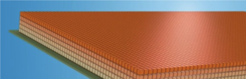
PLANAR (2D) NAND FLASH STRUCTURE
Planar flash cells are placed in a 2-dimensional structure, divided into 2 planes. Odd Flash blocks in plane 0, even in Plane 1. Cells form bytes, bytes form sectors/pages and pages form blocks. Cells are connected to form a grid array, with bit lines and word lines as mentioned above.
Moore’s law predicts a limit to how small the planar process can shrink, before things don’t work anymore. We are about at that limit, with process shrinks smaller than 15nm.
Depiction of 2D FLASH:
As an analogy, given a fixed space, you can only fit so many apartments in a one story building. So, what can be done? The only option is to build up to a multi-level building. If the original building had 100 apartments, and we stack 20, we now have 2000 apartments. There are limits to how many levels are possible.
This is the logic used to create 3D NAND Flash. Of course, production becomes more complicated. There are also limits on the number of stacks.
(3D) NAND FLASH STRUCTURE
3D NAND flash is a type of Flash memory cells that are stacked vertically in multiple layers. Flash manufacturers developed 3D NAND to address challenges they encountered in scaling 2D/planar to achieve higher densities at a lower cost per bit. Planar NAND flash technology uses a single layer of memory cells. As NAND manufacturers worked to shrink the memory cells, cell-to-cell interference caused a reduction in the reliability of planar NAND flash products. 3D NAND flash is suitable for the same types of business and consumer applications for which planar NAND is in use.
With 3D Flash, 2D planes of cells are stacked one on top of the other vertically and layered. Connections between layers are made by rods passing through each layer top to bottom. 32, 64, 48 layers are common. Even 96+ layers are possible. The control logic is relegated to the bottom layer.
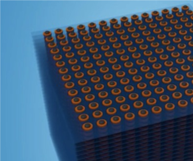
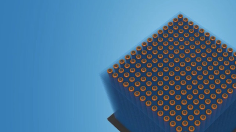
DEPICTIONS OF 3D FLASH ARCHITECTURE-
Rod connecting layers:

Multiple RODS connecting layers:
Control Layer is seen at the bottom of the completed stack:
3D NAND vs. PLANAR NAND
3D NAND flash offers the potential for higher capacity in a smaller physical space than 2D NAND. In comparison to planar NAND, 3D NAND can lower the cost per GB improve electrical use to reduce power consumption, boost reliability, and provide higher write speeds.
One disadvantage of 3D NAND vs. planar NAND is the higher manufacturing cost, at least at the outset. The production of 3D NAND flash can take place in the same factory as planar NAND, but the layering process adds steps to the 3D NAND manufacturing process. Manufacturers often need to update, expand and/or add semiconductor fabs, to accommodate 3D NAND production.
Samsung was the first manufacturer to mass-produce 3D NAND flash, under the name Vertical NAND (V-NAND), in 2013. Other 3D NAND manufacturers include Intel and Micron Technology.
Although manufacturers take different approaches to build 3D NAND flash technology, the methods to read and write data to a 3D NAND cell and a planar NAND cell are essentially the same.
3D NAND TYPES
The main types of NAND flash technology are:
Single-level cell (SLC): Stores 1 bit per cell, offers the highest endurance.
Multi-level cell (MLC): Stores multiple bits per cell, although the term MLC typically equates to 2 bits per cell; provides lower endurance than SLC.
Triple-level cell (TLC): Stores 3 bits per cell, offers lower endurance than SLC and MLC.
3D NAND generally uses MLC NAND flash or TLC NAND flash.
Manufacturers have improved the endurance and reliability of MLC and TLC flash drives through ECC algorithms, wear leveling and other mechanisms. Toshiba, had developed a 96-layer 3D NAND Flash technology with sampling starting in the second half of 2017 and initial production in 2018. The product is based upon the WD/Toshiba BiCS4 architecture. This will be initially deployed in a 256 Gb chip and will eventually ship in a range of capacities, up to 1 Tb on a single chip (that means 8 chips would provide 1 TB storage capacity. This is truly amazing.
All the flash manufacturers are shipping at least 48-layer 3D flash memory and all are shipping or developing 64-layer or higher (in April HK Hynix announced that it has built a 72-layer 3D NAND die with 256 Gb storage capacity, although there appeared no definite schedule for 72-layer chip products).
WD said that it expects that in calendar year 2017, the output mix of its 64-layer 3D NAND technology, BiCS3, will comprise more than 75 percent of its overall 3D NAND bit supply. The company now believes that, along with its partner Toshiba Corporation, the combined 64-layer 3D NAND bit output of the joint ventures in calendar year 2017 will be higher than any other industry.
Just how high could 3D flash memory stacks go? At the 2016 IEDM conference SK Hynix talked about stacking technologies that could enable over 256 memory cell layers. Moving to 3D flash memory has allowed the manufacturing of denser non-volatile memory chips without reducing the lithographic features. The industry had almost reached the limit of how small it could make operating devices lithographic features.
This progress has not been without cost. 3D flash fabs cost considerably more than planar flash fabs and the new manufacturing processes have resulted in yield and other manufacturing ramp issues that have limited the availability of flash memory for the growing flash memory market. By the end of 2017 or early in 2018 we expect that many of these manufacturing ramp issues will be resolved so flash memory can continue to decline in price (flash memory price hikes due to an imbalance of supply and demand has been common throughout 2017).
Advanced development at all the flash memory companies indicates that hundreds of 3D NAND layer structures are possible, but as the height of the stacks increases, there are increased manufacturing issues that impact the manufacturability of high count flash memory stacks.
3D flash stacks are built with holes etched into a stack of memory layers on top of silicon substrates. As these holes get deeper to contain high stack count 3D flash, tapering, hole shape control, and read current control become major challenges.
3D NAND vs. 2D NAND RELIABILITY
PLANAR 2D NAND FLASH:
SLC FLASH: (1 bit per Flash cell) 50K to 100K P/E cycles
MLC FLASH: (2 bits per Flash Cell) 3K to 10K P/E cycles
TLC FLASH: (3 bits per Flash cell) 300 to 1K P/E cycles
3D NAND FLASH:
SLC FLASH: Not Manufactured
MLC FLASH: 30K to 35K P/E cycles
TLC FLASH: 15k to 30K P/E cycles
As seen, the durability of 3D Flash is much better than its 2D counterpart. With proper ECC and wear leveling, the sky is the limit.
In a future article, we will compare the performance of 2D to 3D NAND Flash. Out prediction is 3D Flash will totally replace 2D Flash within the next few years.
Contact
Article Contributor:
Carmine C. Cupani, MSEE
CTech Electronics LLC